Media Summary: Russia is commissioning one of the world's most advanced synchrotron radiation sources — SKIF (Siberian Circular Photon ... Errata: 2:28 - I should make more clear differences between Proximity and Projection This article focuses on the ambitious American startup Substrate, which aims to revolutionize semiconductor manufacturing by ...
X Ray Lithography Presentation - Detailed Analysis & Overview
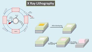
Russia is commissioning one of the world's most advanced synchrotron radiation sources — SKIF (Siberian Circular Photon ... Errata: 2:28 - I should make more clear differences between Proximity and Projection This article focuses on the ambitious American startup Substrate, which aims to revolutionize semiconductor manufacturing by ... You can JOIN US by sign up by clicking on this link. Lecture by Swati Sharma, Indian Institute of Technology Mandi, Himachal Pradesh, India. What does it take to print billions of transistors with nanometer precision? It's a joint effort, one that brings together both hardware ...
Introduction to DXRL by Benedetta Marmiroli: Deep Subject - VLSI Technology Semester - I (M.Tech, Electronics & Telecommunication) University - Chhattisgarh Swami Vivekanand ... Subject:Material Science Paper:Semiconductor material and devices. LEARN MORE: This video lesson was taken from our Subject: Electrical Course: VLSI Technology. Russia is making a bold move in semiconductor technology with its 11.2-nanometer
AKGEC . Do subscribe to the AKGEC channel & get regular ...