Media Summary: As part of MIT's Independent Activities Period (IAP), Mark Mondol, Assistant Director for the Nano Structures Laboratory; and ... NFFA-EUROPE for nanoeducation - lectures and training courses on the specialised technology and fine analysis techniques ... Nanotechnology: A Maker's Course EBL Basics Link to the full Coursera course:

Electron Beam Lithography - Detailed Analysis & Overview

As part of MIT's Independent Activities Period (IAP), Mark Mondol, Assistant Director for the Nano Structures Laboratory; and ... NFFA-EUROPE for nanoeducation - lectures and training courses on the specialised technology and fine analysis techniques ... Nanotechnology: A Maker's Course EBL Basics Link to the full Coursera course: Feel free to WhatsApp us: WhatsAPP @:- +919990880870 Join our Whatsapp Group ... This video is part of the lecture for the course MANU 4344 Micromanufacturing Technology. You can JOIN US by sign up by clicking on this link.

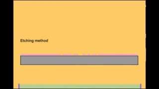
It is one of the process of IC fabrication to remove unwanted layer.  ... photoresist, dark field, bright field mask, exposure, UV, wafer.

Photo Gallery

Electron Beam Lithography
e-Beam Lithography
Drawing Microscopic Patterns with Electrons
A brief introduction to e-beam lithography
Electron beam lithography
Electron Beam Lithography
Nanofabrication Techniques: Electron Beam Lithography
Introduction to EBL
Electron Beam Lithography | VLSI Technology | IC Fabrication
Electron Beam Lithography I EBL I Photolithography | IC Fabrication I VLSI Technology I ESE NET
Lecture 61 (CHE 323) E-Beam Lithography, part 1
Lecture 9 Electron Beam Lithography (EBL)
View Detailed Profile
Electron Beam Lithography

Electron Beam Lithography

How does

e-Beam Lithography

e-Beam Lithography

e-Beam Lithography

Drawing Microscopic Patterns with Electrons

Drawing Microscopic Patterns with Electrons

Today we're looking at

A brief introduction to e-beam lithography

A brief introduction to e-beam lithography

As part of MIT's Independent Activities Period (IAP), Mark Mondol, Assistant Director for the Nano Structures Laboratory; and ...

Electron beam lithography

Electron beam lithography

Electron beam lithography

Electron Beam Lithography

Electron Beam Lithography

Electron beam lithography

Nanofabrication Techniques: Electron Beam Lithography

Nanofabrication Techniques: Electron Beam Lithography

NFFA-EUROPE for nanoeducation - lectures and training courses on the specialised technology and fine analysis techniques ...

Introduction to EBL

Introduction to EBL

Nanotechnology: A Maker's Course EBL Basics Link to the full Coursera course: https://www.coursera.org/learn/nanotechnology ...

Electron Beam Lithography | VLSI Technology | IC Fabrication

Electron Beam Lithography | VLSI Technology | IC Fabrication

Electron Beam Lithography

Electron Beam Lithography I EBL I Photolithography | IC Fabrication I VLSI Technology I ESE NET

Electron Beam Lithography I EBL I Photolithography | IC Fabrication I VLSI Technology I ESE NET

Feel free to WhatsApp us: WhatsAPP @:- +919990880870 Join our Whatsapp Group ...

Lecture 61 (CHE 323) E-Beam Lithography, part 1

Lecture 61 (CHE 323) E-Beam Lithography, part 1

Electron Beam Lithography

Lecture 9 Electron Beam Lithography (EBL)

Lecture 9 Electron Beam Lithography (EBL)

This video is part of the lecture for the course MANU 4344 Micromanufacturing Technology.

Making Tiny Things with Electron Microscope - E-beam Lithography

Making Tiny Things with Electron Microscope - E-beam Lithography

More info: http://sam.zeloof.xyz/

E-Beam Lithography, Part 1

E-Beam Lithography, Part 1

E

mod03lec08 - Device Fabrication-Electron-beam Lithography

mod03lec08 - Device Fabrication-Electron-beam Lithography

Device Fabrication-

Electron Beam Lithography (Hindi) | Micro Machining

Electron Beam Lithography (Hindi) | Micro Machining

You can JOIN US by sign up by clicking on this link.

E-beam lithography at DTU Nanolab

E-beam lithography at DTU Nanolab

DTU Nanolab has a JEOL 9500FS

''Electron Beam LITHOGRAPHY'' VLSI TECHNOLOGY By Ms  Pragya Srivastava, AKGEC

''Electron Beam LITHOGRAPHY'' VLSI TECHNOLOGY By Ms Pragya Srivastava, AKGEC

It is one of the process of IC fabrication to remove unwanted layer. #AKGEC #AKGECGhaziabad #BestEngineeringCollege ...

Lec 27 Lithography

Lec 27 Lithography

photoresist, dark field, bright field mask, exposure, UV, wafer.

Next Generation Lithography : DSA, E-beam

Next Generation Lithography : DSA, E-beam

Next generation