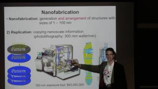
Media Summary: Dr. David Lam of Multibeam Corporation describes the misperceptions and opportunities for As part of MIT's Independent Activities Period (IAP), Mark Mondol, Assistant Director for the Nano Structures Laboratory; and ... Aki Fujimura, CEO of D2S, sat down with Semiconductor Engineering to talk about the challenges of moving to the

Next Generation Lithography Dsa E Beam - Detailed Analysis & Overview

Dr. David Lam of Multibeam Corporation describes the misperceptions and opportunities for As part of MIT's Independent Activities Period (IAP), Mark Mondol, Assistant Director for the Nano Structures Laboratory; and ... Aki Fujimura, CEO of D2S, sat down with Semiconductor Engineering to talk about the challenges of moving to the The march to the next node will depend on overcoming barriers and exploiting multiple solutions before " Subject:Physics Course:Quantum Transport. Time lapse video of a recent equipment installation project at University of Bristol, where we helped School of Physics with moving ...

Photo Gallery

Next Generation Lithography : DSA, E-beam
Electron Beam Lithography
Next Generation Lithography : Nanoimprint
Tech Talk: Multicolumn eBeam Lithography (MEBL)
Ep11 Nanofabrication, e-beam and photolithography, Moore's law. UCSD, NANO 11/101, Darren Lipomi
A brief introduction to e-beam lithography
Making Tiny Things with Electron Microscope - E-beam Lithography
Next-Generation Lithography
The #1 challenge of EUV lithography | ASML
E-beam lithography at DTU Nanolab
Drawing Microscopic Patterns with Electrons
Electron Beam Lithography with NPGS Tutorial (Qubit Gate Layer)
View Detailed Profile
Next Generation Lithography : DSA, E-beam

Next Generation Lithography : DSA, E-beam

Next generation lithography

Electron Beam Lithography

Electron Beam Lithography

How does

Next Generation Lithography : Nanoimprint

Next Generation Lithography : Nanoimprint

Next generation lithography

Tech Talk: Multicolumn eBeam Lithography (MEBL)

Tech Talk: Multicolumn eBeam Lithography (MEBL)

Dr. David Lam of Multibeam Corporation describes the misperceptions and opportunities for

Ep11 Nanofabrication, e-beam and photolithography, Moore's law. UCSD, NANO 11/101, Darren Lipomi

Ep11 Nanofabrication, e-beam and photolithography, Moore's law. UCSD, NANO 11/101, Darren Lipomi

Nanofabrication,

A brief introduction to e-beam lithography

A brief introduction to e-beam lithography

As part of MIT's Independent Activities Period (IAP), Mark Mondol, Assistant Director for the Nano Structures Laboratory; and ...

Making Tiny Things with Electron Microscope - E-beam Lithography

Making Tiny Things with Electron Microscope - E-beam Lithography

More info: http://sam.zeloof.xyz/

Next-Generation Lithography

Next-Generation Lithography

Aki Fujimura, CEO of D2S, sat down with Semiconductor Engineering to talk about the challenges of moving to the

The #1 challenge of EUV lithography | ASML

The #1 challenge of EUV lithography | ASML

What's the most difficult hurdle in EUV

E-beam lithography at DTU Nanolab

E-beam lithography at DTU Nanolab

DTU Nanolab has a JEOL 9500FS

Drawing Microscopic Patterns with Electrons

Drawing Microscopic Patterns with Electrons

Today we're looking at

Electron Beam Lithography with NPGS Tutorial (Qubit Gate Layer)

Electron Beam Lithography with NPGS Tutorial (Qubit Gate Layer)

Demo of

Lecture 61 (CHE 323) E-Beam Lithography, part 1

Lecture 61 (CHE 323) E-Beam Lithography, part 1

Electron Beam Lithography

Yan Borodovsky: The various paths to next-generation lithography

Yan Borodovsky: The various paths to next-generation lithography

The march to the next node will depend on overcoming barriers and exploiting multiple solutions before "

Device Fabrication-Electron-beam Lithography

Device Fabrication-Electron-beam Lithography

Subject:Physics Course:Quantum Transport.

Installation of Raith Voyager - Electron Beam Lithography tool at University of Bristol

Installation of Raith Voyager - Electron Beam Lithography tool at University of Bristol

Time lapse video of a recent equipment installation project at University of Bristol, where we helped School of Physics with moving ...

The Strategic Positioning of Electron Beam Lithography

The Strategic Positioning of Electron Beam Lithography

Web site story link: http://www.thomasdalejay.blogspot.com/2013/05/the-strategic-positioning-of-