Media Summary: FormFactor's ReAlign™ technology for the SUMMIT200 Subscribe it to get more information! Camera Module System Semiconductor System www.techinspirit.co.kr. What is the process by which silicon is transformed into a semiconductor chip? As the second most prevalent material on earth, ...

Wafer Probing - Detailed Analysis & Overview

FormFactor's ReAlign™ technology for the SUMMIT200 Subscribe it to get more information! Camera Module System Semiconductor System www.techinspirit.co.kr. What is the process by which silicon is transformed into a semiconductor chip? As the second most prevalent material on earth, ... Watch How are BILLIONS of MICROCHIPS made from SAND? How are SILICON This video shows how these tests are carried out using Polytec's MSA Micro System Analyzer interfaced to a Whether that's at +150 degrees C (or higher) or at sub-freezing temperatures,

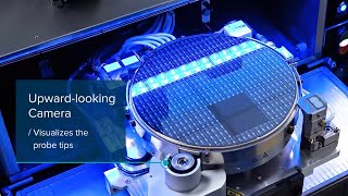
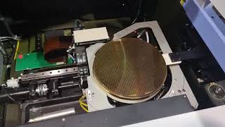
Automated wafer probing with vertical probe cards on the summit200 probe station - FORMFACTOR Kindly send us your detailed requirements Email: sales01.com , WhatsApp: Nicole +86 15889675465. Dive into the intricate world of foundries with Advantest experts Keith Schaub and Shinji Hioki, as Shinji shares his extensive ... The Velox™ Workflow Guide helps users perform accurate measurements on FormFactor

Photo Gallery

Automated Wafer Probing with Vertical Probe Cards on the SUMMIT200 Probe Station – FormFactor
MIMOS Failure Analysis - Wafer Level Testing
(Wafer Series) WAFER PROBE SYSTEM
Wafer Probing
‘Semiconductor Manufacturing Process’ Explained | 'All About Semiconductor' by Samsung Semiconductor
How are BILLIONS of MICROCHIPS made from SAND? | How are SILICON WAFERS made?
Wafer-Level and Single-Die Testing
Semiconductor testing
What is a probe card (in 120 seconds) - Technoprobe
Mechanical and Temperature Probing Challenges - FormFactor
Automated wafer probing with vertical probe cards on the summit200 probe station - FORMFACTOR
Wafer Prober Automatic Probe-to-Pad Alignment
View Detailed Profile
Automated Wafer Probing with Vertical Probe Cards on the SUMMIT200 Probe Station – FormFactor

Automated Wafer Probing with Vertical Probe Cards on the SUMMIT200 Probe Station – FormFactor

FormFactor's ReAlign™ technology for the SUMMIT200

MIMOS Failure Analysis - Wafer Level Testing

MIMOS Failure Analysis - Wafer Level Testing

Wafer testing

(Wafer Series) WAFER PROBE SYSTEM

(Wafer Series) WAFER PROBE SYSTEM

Subscribe it to get more information! Camera Module System Semiconductor System www.techinspirit.co.kr.

Wafer Probing

Wafer Probing

An engineer using one of our

‘Semiconductor Manufacturing Process’ Explained | 'All About Semiconductor' by Samsung Semiconductor

‘Semiconductor Manufacturing Process’ Explained | 'All About Semiconductor' by Samsung Semiconductor

What is the process by which silicon is transformed into a semiconductor chip? As the second most prevalent material on earth, ...

How are BILLIONS of MICROCHIPS made from SAND? | How are SILICON WAFERS made?

How are BILLIONS of MICROCHIPS made from SAND? | How are SILICON WAFERS made?

Watch How are BILLIONS of MICROCHIPS made from SAND? | How are SILICON

Wafer-Level and Single-Die Testing

Wafer-Level and Single-Die Testing

This video shows how these tests are carried out using Polytec's MSA Micro System Analyzer interfaced to a

Semiconductor testing

Semiconductor testing

From

What is a probe card (in 120 seconds) - Technoprobe

What is a probe card (in 120 seconds) - Technoprobe

What does Technoprobe do?

Mechanical and Temperature Probing Challenges - FormFactor

Mechanical and Temperature Probing Challenges - FormFactor

Whether that's at +150 degrees C (or higher) or at sub-freezing temperatures,

Automated wafer probing with vertical probe cards on the summit200 probe station - FORMFACTOR

Automated wafer probing with vertical probe cards on the summit200 probe station - FORMFACTOR

Automated wafer probing with vertical probe cards on the summit200 probe station - FORMFACTOR

Wafer Prober Automatic Probe-to-Pad Alignment

Wafer Prober Automatic Probe-to-Pad Alignment

APEX 200mm

Wafer Probe

Wafer Probe

Wafer Probe

Wafer testing

Wafer testing

Kindly send us your detailed requirements Email: sales01@jinfly.com , WhatsApp: Nicole +86 15889675465.

Next-Generation Electro-Optical Wafer Probing with a Scalable Technology Platform

Next-Generation Electro-Optical Wafer Probing with a Scalable Technology Platform

Our photonic

Wafer Testing Secrets You Did Not Know Yet

Wafer Testing Secrets You Did Not Know Yet

Dive into the intricate world of foundries with Advantest experts Keith Schaub and Shinji Hioki, as Shinji shares his extensive ...

TSK UF200 PROBER WAFER DUMMY TEST

TSK UF200 PROBER WAFER DUMMY TEST

Used TSK UF200 PROBER for sale -

TSK UF3000 PROBER WAFER DUMMY TEST

TSK UF3000 PROBER WAFER DUMMY TEST

Used TSK UF3000 PROBER for sale -

Velox™ Workflow Guide for Guided Wafer Probing | FormFactor

Velox™ Workflow Guide for Guided Wafer Probing | FormFactor

The Velox™ Workflow Guide helps users perform accurate measurements on FormFactor