Media Summary: Get ten 100x100mm one or two layer high quality Video explain the easy procedure for converting pcb circuit cloning tracing design for made DIY circuit any type of pcb so you try this application sprint layout 6.0 use ...
Reverse Pcb Design Tracing - Detailed Analysis & Overview
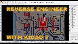
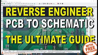
Get ten 100x100mm one or two layer high quality Video explain the easy procedure for converting pcb circuit cloning tracing design for made DIY circuit any type of pcb so you try this application sprint layout 6.0 use ... Welcome to this tutorial on using KiCAD for For best development boards / components shop here : ** After creating the "COPPER FILL ZONE" with ... Powered by Restream Eric Schlaepfer shows us techniques for
So you have a PCB and no Schematic - here one method you can use to